The two (2) models of the deviceWISE SmartIO Signal Interface Unit can easily be equipped with simple loopback test harness circuits to experiment with and validate the functionality of the deviceWISE SmartIO driver and event handlers. As the ADSC1 unit supports two (2) 0 - 20 mAmp analog inputs, four (4) digital inputs, two (2) digital outputs, and two (2) hardware counters, we can connect loop back circuits between the digital output and digital input signals. Similarly, using fixed resister circuits, we can supply steady analog input values to the two (2) 0 - 20 mAmp analog input channels.
In a similar manner, as the DS11 unit supports eight (8) digital inputs and eight (8) digital outputs, we can connect loop back circuits between the digital output and digital input signals.
Using this loopback methodology, we can drive the digital input signals programmatically using the digital outputs.
Creating an ADSC1 Test Harness Circuit Configuration
The circuit schematic diagram below shows how to create a test harness for the ADSC1 signal interface unit.
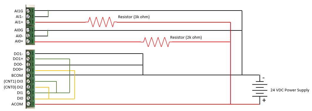
In most cases, the same 24 VDC power supply being used to power the signal interface unit can be used to power the test harness circuit.
This test harness configuration will allow the user to energize the DI0 and DI2 inputs using the DO0 output. On the rising signal edge, tranisition zero (0) to one (1), off to on, the change in DI2 will cause hardware counter CNT0 to increment. This test harness configuration will also allow the user to energize the DI1 and DI3 inputs using the DO1 output. On the rising signal edge, tranisition zero (0) to one (1), off to on, the change in DI3 will cause hardware counter CNT1 to increment.
The use of the 3k ohm resister will generate a steady 8 milliamp signal and the use of the 2k ohm resister will generate a steady 12 milliamp signal when using a 24 VDC power source.
The SmartIO driver presents the 12-bit digitized analog value. What this represents is a value of 0 - 4095 to represent the physical electrical signal of 0 - 20 milliamps of current.
As such, calculations are simply made as… mAmp = (value / 4096) * 20.
Creating a DS11 Test Harness Circuit Configuration
The circuit schematic diagram below shows how to create a test harness for the DS11 signal interface unit.
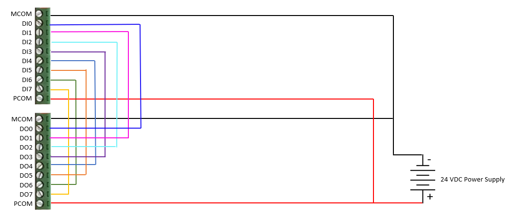
The DS11 unit requires an external power source to drive the digitial input and output signals. In most cases, the same 24 VDC power supply being used to power the signal interface unit can be used to power the test harness circuit.
This test harness configuration will allow the user to energize the DO0 and send an input signal to DI0… the same is true for all eight (8) channels such that energizing DOn will send a signal to DIn.